自己编写处理器-Verilog设计实现MU0处理器
MU0是一个基础的16位单流水线通用可编程处理器,具有16位的数据总线和12位地址总线。本篇主要使用Verilog的行为描述方法编程实现MU0的设计,主要包含Control和Datapath两部分,两个主要模块相互配合实现处理器的基本功能。
设计来源:UoM
文章大纲
接口设计
话不多说,先来看总体的接口设计图。
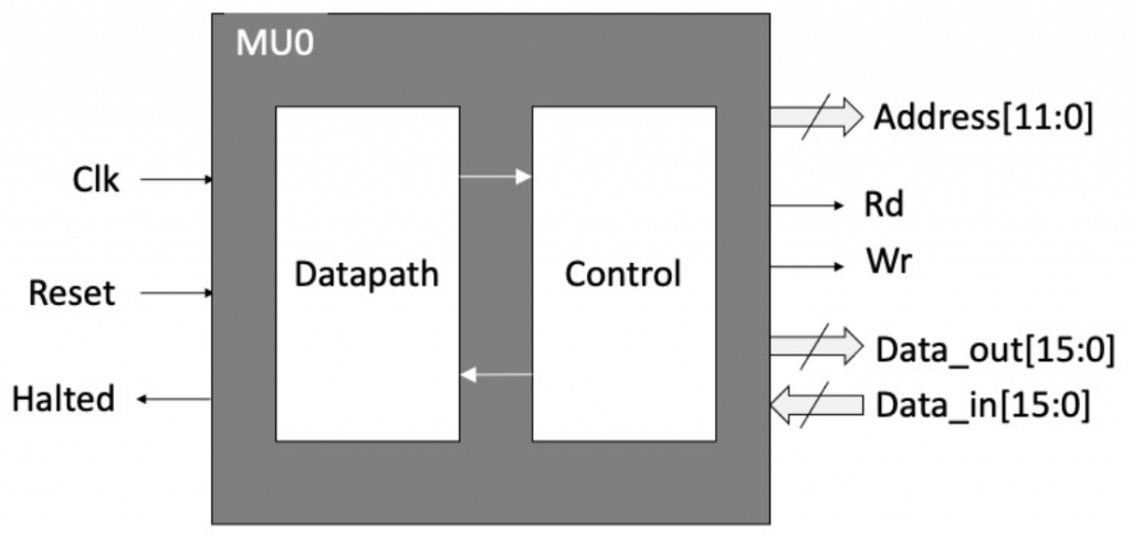
外部输入信号包括:
- Clk:时钟信号
- Reset:重置(初始化)信号
- Data_in:16位数据总线(输入)
输出信号有:
- Data_out:16位数据总线(输出)
- Address:12位地址总线(地址总线的宽度小于数据总线是为了简化设计)
- Rd:读信号,指示读取地址总线指向的内存中的数据到输入数据总线中。
- Wr:写信号,指示将输出数据总线上的数据写入到地址总线指向的内存中。(注:Rd和Wr不可同时为高位)
- Halted:用于指示MU0处于停止状态
指令格式和功能描述
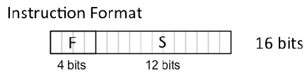
作为通用可编程处理器,指令是MU0的灵魂所在。MU0使用基于累加器的单地址指令集架构,其指令由定长的16位组成,其中前4位作为指令编码,后12位为操作数的内存地址。这样一来,显操作数被指定在指令中,而累加器作为第二个隐操作数参与计算。MU0以直接内存访问的方式获取指令操作数,因12位的内存地址得以将其直接完整编码进指令中,极大简化了指令设计。
在描述具体指令之前,首先需要了解MU0的两个十分重要的寄存器。16位的累加器ACC:作为另一个隐操作数参与到指令的执行中;12位的程序计数器PC:用于指示下一条指令所在的内存地址,默认情况下,初始指令位于内存地址0值处。它们也是MU0中仅有的两个“对用户可见”的寄存器。
MU0具体支持的指令和功能描述见下表:
| 指令编码 | 助记符 | 功能描述 |
| 0000 | LDA S | 读取,将内存地址S中的数据读取到累加器。 |
| 0001 | STA S | 写入,将累加器中的数据写入到内存地址S。 |
| 0010 | ADD S | 加法运算,将内存地址S中的值加到累加器中。 |
| 0011 | SUB S | 减法运算,从累加器中减去内存地址S中的值。 |
| 0100 | JMP S | 跳转,跳转至指令地址S。 |
| 0101 | JGE S | 条件跳转,如果累加器中的值大于或等于0则跳转。 |
| 0110 | JNE S | 条件跳转,如果累加器中的值非0则跳转。 |
| 0111 | STP | 停止指令,停止处理器继续运行。 |
| 1000-1111 | – | 保留编码,未使用。 |
Datapath设计
实际设计阶段开始,先看Datapath部分。Datapath如名“数据路径”,描述了处理器内部各个模块的组合方式,定义数据的传播,其实现了FSM所需的数据操作功能,是基于寄存器的组合设计,主要使用结构化设计。来看设计图。
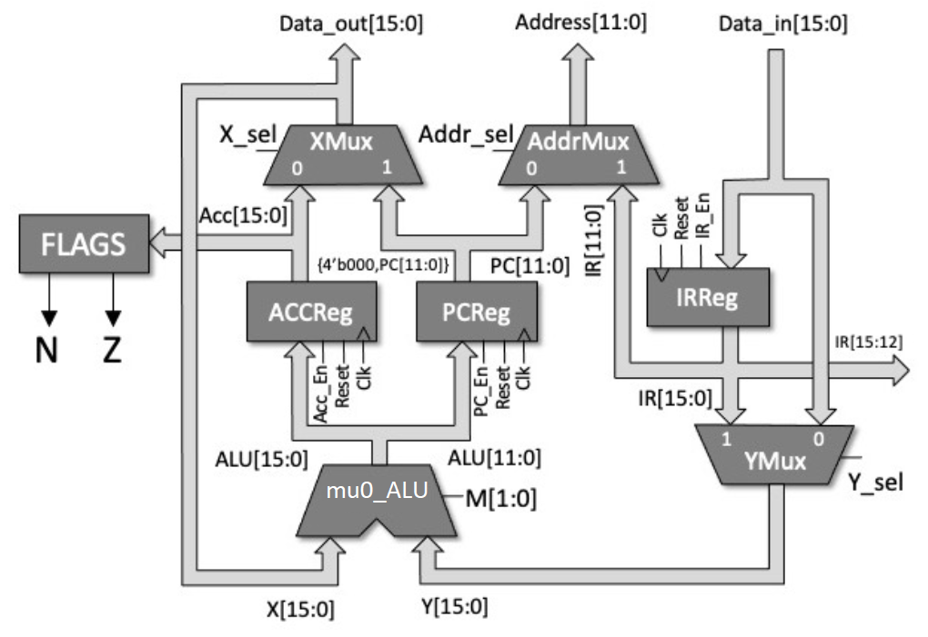
内部模块大致可以分为四类。
- 2选1多路复用器 – 分为12位和16位两种。其中
XMux和YMux因各自连接不同的数据总线,为16位;AddrMux连接地址总线,为12位。 - 寄存器 – 同样分为12位和16位。IRReg为指令寄存器,存储当前执行的指令,为16位;ACCReg为累加器,16位;PCReg为程序计数器,存储下一条指令内存地址,为12位。
- ALU算术逻辑单元 – 这一部分的详细内容参见之前的文章ALU算术逻辑单元。
- 标志位模块 – 根据累加器的值输出标志位信号N(负值)和Z(零值)。
12位/16位2选1多路复用器Verilog行为设计代码:
module mu0_mux12(input  wire [11:0] A,
			input  wire [11:0] B,
			input  wire        S,
			output reg  [11:0] Q);

// Combinatorial logic for 2to1 multiplexor
// S is select, A channel0, B channel1
always @ (*)
case (S)
	1'b0:	Q = A;
	1'b1:	Q = B;
	default:	Q = 12'hXXX;
endcase
endmodule

module mu0_mux16(input  wire  [15:0] A,
			input  wire  [15:0] B,
			input  wire         S,
			output reg  [15:0]  Q);

// Combinatorial logic for 2to1 multiplexor
// S is select, A channel0, B channel1
always @ (*)
case (S)
	1'b0:	Q = A;
	1'b1:	Q = B;
	default:	Q = 16'hXXXX;
endcase
endmodule
12位/16位寄存器是时钟同步驱动的,并设有重置信号,Verilog行为设计代码:
module mu0_reg12(input  wire        Clk,
			input  wire        Reset,
			input  wire        En,
			input  wire [11:0] D,
			output reg  [11:0] Q);

// behavioural code - clock driven
always @ (posedge Clk, posedge Reset)
if (Reset)
	// reset
	Q <= 12'h000;
else if (En)
	// update Q when En is high
	Q <= D;

endmodule

module mu0_reg16(input  wire        Clk,
			input  wire        Reset,
			input  wire        En,
			input  wire [15:0] D,
			output reg  [15:0] Q);

// behavioural code - clock driven
always @ (posedge Clk, posedge Reset)
if (Reset)
	// reset
	Q <= 16'h0000;
else if (En)
	// update Q when En is high
	Q <= D;

endmodule
标志位模块根据累加器中的值输出标志位,若值为负则N为1,若值为0则Z为1,标志位信号实际上为条件跳转指令提供判断的依据,Verilog行为设计代码:
module mu0_flags(input  wire [15:0]  Acc,
			output reg          N,
			output reg          Z);

// Combinatorial logic
always @(*)
 begin
   Z = ~|Acc;     // When Acc equals 0, Zero flag is set
   N = Acc[15];   // When negative bit of Acc is set, Negative flag is set
 end

endmodule
下面分析Datapath的输入输出信号。
输入信号(MU0控制信号):
- Clk:时钟信号,使用统一的时钟同步更新所有寄存器来更新系统的状态。
- Reset:重置信号,接收到高电平时重置寄存器的值。
- Data_in:16位输入数据总线。
- X_sel:XMux的选择信号。
- Y_sel:YMux的选择信号。
- Addr_sel:AddrMux的选择信号。
- PC_En:控制PCReg是否处于激活状态,只有处于激活状态时寄存器才能进行数据读写。
- IR_En:控制IRReg是否处于激活状态。
- Acc_En:控制ACCReg是否处于激活状态。
- M:控制ALU的工作模式,两位。
输出信号:
- F:指令数据的前四位,即指令编码。
- Address:12位地址总线。
- Data_out:16位输出数据总线。
- N:标志位负值信号。
- Z:标志位零值信号。
除此以外,Datapath中还需要许多内部信号来连接内部各模块,参见设计图,这里不再一一列出。
到此,根据原设计图,可以很容易的完成整个Datapath部分的Verilog结构设计代码:
module mu0_datapath(input  wire        Clk,
			input  wire        Reset,
			input  wire [15:0] Data_in,
			input  wire        X_sel,
			input  wire        Y_sel,
			input  wire        Addr_sel,
			input  wire        PC_En,
			input  wire        IR_En,
			input  wire        Acc_En,
			input  wire [1:0]  M,
			output wire [3:0]  F,			// top 4 bits of the instruction
			output wire [11:0] Address,
			output wire [15:0] Data_out,
			output wire        N,
			output wire        Z);

// Internal signals for datapath schematic
wire [11:0] PC;
wire [15:0] IR, ALU, Acc, X, Y;

// Instantiate Datapath components
// Uses explicit dot pins - safer than position substitution

//MU0 registers
mu0_reg12 PCReg(Clk, Reset, PC_En, ALU[11:0], PC);
mu0_reg16 IRReg(Clk, Reset, IR_En, Data_in, IR);
mu0_reg16 ACCReg(Clk, Reset, Acc_En, ALU, Acc);

// MU0 multiplexors
mu0_mux16 XMux(Acc, {4'h0,PC}, X_sel, X);
mu0_mux16 YMux(Data_in, IR, Y_sel, Y);
mu0_mux12 AddrMux(PC, IR[11:0], Addr_sel, Address);

// MU0 ALU
mu0_alu mu0_ALU(X, Y, M, ALU);

// MU0 Flag generation
mu0_flags FLAGS(Acc, N, Z);

// Buffer added to take care od X and Data_out are the same
buf DOUTBuf[15:0] (Data_out, X);
// Buffer added F is op 4 bits of the instruction
buf FBuf[3:0] (F, IR[15:12]);

endmodule
Datapath完成!
Control设计
Control模块负责MU0处理器的状态转换,以及为Datapath提供的正确配置,以使其执行相应数据运算,完成指定的工作。Control中主要包含两个子模块分别对应上述工作,有限状态机(FSM)和解码器(Decode)。
先来看总体设计图。
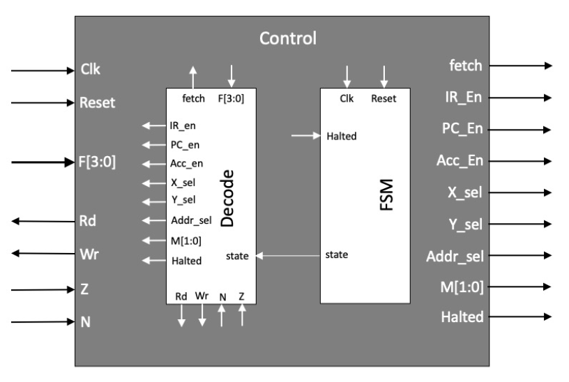
外围的整体输入输出大部分用于连接Datapath与其交互,控制其状态的转变,使Datapath能够执行某一特定状态下所需的功能。大部分信号和之前提到过的一致,这里不再一一解释。解释几个新出现的信号:
- fetch:指示FSM的当前状态,当处于
fetch阶段时为高电平。 - Halted:指示处理器处于停止运行状态,通常由STP指令触发。
工作流程
MU0作为一个单流水线处理器,每一条指令的读取和执行的过程作为一个完整的周期,其中可简化抽象为取址和解码/执行两个状态,每个状态占据一个独立的时钟周期,因此一条指令的执行总共消耗两个时钟周期。正常情况下指令的执行会在两个状态间切换运行,在一条指令执行结束后进行下一条指令的取址工作。直到执行到STP指令,处理器停止运行,并停留在执行状态。
绘制出状态转换示意图如下:
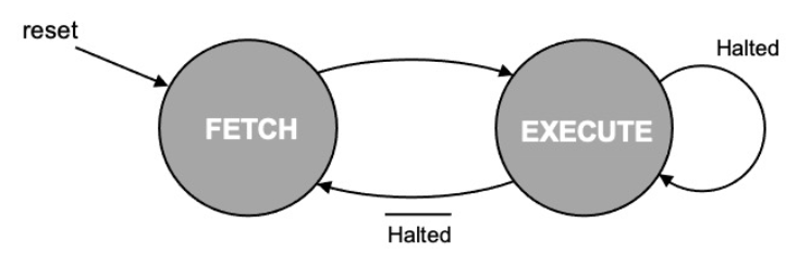
在取址(fetch)状态,完成取址和解码两项任务。首先根据PC程序计数器中的地址值取址,即输出PC的值到地址总线上,并设置读信号Rd为1,于是读取输入数据总线的数据至IR指令寄存器。与此同时,更新PC,将PC程序计数器指向下一条待执行的指令地址,即通过ALU执行+1运算,顺序指向下一条指令。
在执行(execute)状态,首先,对IR指令寄存器中的指令进行解码,拆分出指令编码(前4位)和内存操作数地址(后12位);根据得到的内存操作数地址,从内存中获取操作数;再根据具体的指令编码,对操作数执行相应的指令操作,如LDA加载累加器或JMP更新PC程序计数器等等,其中最为关键的所有数值计算任务将通过ALU来完成;最后写入结果,依据不同的指令,执行的输出结果可能会被存储至寄存器(如ADD指令)或写入内存(如STA指令)中。
需要注意的是,在上述状态内,部分工作的执行存在逻辑上的先后顺序,但仍可以组织在同一状态中,这是因为这些工作的执行发生在处理器内部彼此没有任何影响,因此只需保证在单个时钟周期内所有的工作都能完成(时钟周期>关键路径),即可确保最终结果的正确性。
FSM有限状态机
FSM控制MU0的状态转换,其处理逻辑很简单,随时钟周期切换状态即可。其中,下一状态的计算取决于当前状态和外部信号(如Halted)输入。注意这里的FSM与传统的有限状态机相比,没有输出计算部分,只有当前状态转换和下一状态计算,这是因为输出计算的工作由于较为复杂,已经整合入Decode模块,单独作为一个大模块执行。
编写FSM的Verilog行为设计代码:
module mu0_fsm(input  wire         Clk,
			input  wire         Reset,
			input  wire    Halted,
			output reg          state);
// internal variables
reg next_state;

// Behavioural description
// determine the next state
always @ (*)
begin
	case (state)
		1'b0:	next_state = 1'b1;
		1'b1:	if (Halted)	next_state = 1'b1;
				else		next_state = 1'b0;
		default:	next_state = 1'bx;
	endcase
end

// perform the assignment to current state
always @ (posedge Clk, posedge Reset)
begin
	if (Reset)
		state <= 1'b0;
	else
		state <= next_state;
end

endmodule
Decode解码器
解码器根据不同状态以及execute状态下的不同指令设置各个输出信号,这些信号中主要包含了Datapath所需的控制信号来控制Datapath的正确运作,以完成具体状态或指令的执行。需要设置的控制信号包括控制寄存器的激活、多路复用器的选择、ALU的工作模式和数据的输入输出等。
结合Datapath的设计图和指令的功能描述表,总结各指令的功能需求和操作逻辑,编写出解码器的Verilog行为设计代码:
module mu0_decode(input  wire        state,      // System clock
                  input  wire [3:0]  F,          // Bits [15:12] of the IR
                  input  wire        N,          // Negative flag
                  input  wire        Z,          // Zero flag
                  output reg         fetch,      // Used for debug
                  output reg         PC_En,      // Update PC
                  output reg         IR_En,      // Update IR
                  output reg         Acc_En,     // Update Acc
                  output reg         X_sel,      // Data Out mux(X port on ALU) 0 for Acc, 1 for PC
                  output reg         Y_sel,      // mux, Y port on ALU, 0 for Data In, 1 for Instr
                  output reg         Addr_sel,   // mux, 0 for PC, 1 for IR
                  output reg  [1:0]  M,          // ALU op, 0) Y, 1) X+Y, 2) X+1, 3) X-Y
                  output reg         Rd,         // Memory read
                  output reg         Wr,         // Memory write
                  output reg         Halted);    // MU0 stopped

// Control decode
always @ (*)
begin
	case (state)
		1'b0:  // fetch
		begin
			fetch = 1'b1;
			PC_En = 1'b1;
			IR_En = 1'b1;
			Acc_En = 1'b0;
			M = 2'b10;
			X_sel = 1'b1;
			Y_sel = 1'bX;
			Addr_sel = 1'b0;
			Rd = 1'b1;
			Wr = 1'b0;
			Halted = 1'b0;
		end
		1'b1:  // execute
		begin
			fetch = 1'b0;
			case (F)
				4'b0000:	//LDA
				begin
					PC_En = 1'b0;
					IR_En = 1'b0;
					Acc_En = 1'b1;
					M = 2'b00;
					X_sel = 1'bX;
					Y_sel = 1'b0;
					Addr_sel = 1'b1;
					Rd = 1'b1;
					Wr = 1'b0;
					Halted = 1'b0;
				end
				4'b0001:	//STA
				begin
					PC_En = 1'b0;
					IR_En = 1'b0;
					Acc_En = 1'b0;
					M = 2'bXX;
					X_sel = 1'b0;
					Y_sel = 1'bX;
					Addr_sel = 1'b1;
					Rd = 1'b0;
					Wr = 1'b1;
					Halted = 1'b0;
				end
				4'b0010:	//ADD
				begin
					PC_En = 1'b0;
					IR_En = 1'b0;
					Acc_En = 1'b1;
					M = 2'b01;
					X_sel = 1'b0;
					Y_sel = 1'b0;
					Addr_sel = 1'b1;
					Rd = 1'b1;
					Wr = 1'b0;
					Halted = 1'b0;
				end
				4'b0011:	//SUB
				begin
					PC_En = 1'b0;
					IR_En = 1'b0;
					Acc_En = 1'b1;
					M = 2'b11;
					X_sel = 1'b0;
					Y_sel = 1'b0;
					Addr_sel = 1'b1;
					Rd = 1'b1;
					Wr = 1'b0;
					Halted = 1'b0;
				end
				4'b0100:	//JMP
				begin
					PC_En = 1'b1;
					IR_En = 1'b0;
					Acc_En = 1'b0;
					M = 2'b00;
					X_sel = 1'bX;
					Y_sel = 1'b1;
					Addr_sel = 1'bX;
					Rd = 1'b0;
					Wr = 1'b0;
					Halted = 1'b0;
				end
				4'b0101:	//JGE
					if (N)  // N==1, do not jump
					begin
						PC_En = 1'b0;
						IR_En = 1'b0;
						Acc_En = 1'b0;
						M = 2'bXX;
						X_sel = 1'bX;
						Y_sel = 1'bX;
						Addr_sel = 1'bX;
						Rd = 1'b0;
						Wr = 1'b0;
						Halted = 1'b0;
					end
					else  // N==0, jump
					begin
						PC_En = 1'b1;
						IR_En = 1'b0;
						Acc_En = 1'b0;
						M = 2'b00;
						X_sel = 1'bX;
						Y_sel = 1'b1;
						Addr_sel = 1'bX;
						Rd = 1'b0;
						Wr = 1'b0;
						Halted = 1'b0;
					end
				4'b0110:	//JNE
					if (Z)  // Z==1, do not jump
					begin
						PC_En = 1'b0;
						IR_En = 1'b0;
						Acc_En = 1'b0;
						M = 2'bXX;
						X_sel = 1'bX;
						Y_sel = 1'bX;
						Addr_sel = 1'bX;
						Rd = 1'b0;
						Wr = 1'b0;
						Halted = 1'b0;
					end
					else  // Z==0, jump
					begin
						PC_En = 1'b1;
						IR_En = 1'b0;
						Acc_En = 1'b0;
						M = 2'b00;
						X_sel = 1'bX;
						Y_sel = 1'b1;
						Addr_sel = 1'bX;
						Rd = 1'b0;
						Wr = 1'b0;
						Halted = 1'b0;
					end
				4'b0111:	//STP
				begin
					PC_En = 1'b0;
					IR_En = 1'b0;
					Acc_En = 1'b0;
					M = 2'bXX;
					X_sel = 1'bX;
					Y_sel = 1'bX;
					Addr_sel = 1'bX;
					Rd = 1'b0;
					Wr = 1'b0;
					Halted = 1'b1;
				end
				default:	// undefined instruction
				begin
					PC_En = 1'b0;
					IR_En = 1'b0;
					Acc_En = 1'b0;
					M = 2'bXX;
					X_sel = 1'bX;
					Y_sel = 1'bX;
					Addr_sel = 1'bX;
					Rd = 1'b0;
					Wr = 1'b0;
					Halted = 1'b0;
				end
			endcase
		end
		default:	// undefined state
		begin
			fetch = 1'bX;
			PC_En = 1'b0;
			IR_En = 1'b0;
			Acc_En = 1'b0;
			M = 2'bXX;
			X_sel = 1'bX;
			Y_sel = 1'bX;
			Addr_sel = 1'bX;
			Rd = 1'b0;
			Wr = 1'b0;
			Halted = 1'b0;
		end
	endcase
end

endmodule
完成Control Block
现在,组合FSM和Decode来完成完整的控制模块的设计。编写Verilog结构设计代码:
module mu0_control(input  wire         Clk,      // System clock
                   input  wire         Reset,    // System reset
                   input  wire  [3:0]  F,        // Bits [15:12] of the IR
                   input  wire         N,        // Negative flag
                   input  wire         Z,        // Zero flag
                   output wire          fetch,    // Used for debug
                   output wire          PC_En,    // Update PC
                   output wire          IR_En,    // Update IR
                   output wire          Acc_En,   // Update Acc
                   output wire          X_sel,    // Data Out mux(X port on ALU) 0 for Acc, 1 for PC
                   output wire          Y_sel,    // mux, Y port on ALU, 0 for Data In, 1 for Instr
                   output wire          Addr_sel, // mux, 0 for PC, 1 for IR
                   output wire   [1:0]  M,        // ALU op, 0) Y, 1) X+Y, 2) X+1, 3) X-Y
                   output wire          Rd,       // Memory read
                   output wire          Wr,       // Memory write
                   output wire          Halted);  // MU0 stopped

//Internal signals
wire state;

// Instantiate MU0 FSM
// Uses explicit dot pins - safer than position substitution
mu0_fsm fsm(Clk, Reset, Halted, state);

// Instantiate Control decode
mu0_decode decode(state, F, N, Z, fetch, PC_En, IR_En, Acc_En, X_sel, Y_sel, Addr_sel, M, Rd, Wr, Halted);

endmodule
至此,MU0处理器的所有模块已经编写完成。最后,让我们完成MU0的最终设计!
组装MU0
I have a Datapath, I have a Control~~ Ah, MU0!
使用编写好的Datapath和Control模块,完成MU0的最终设计。编写Verilog结构设计代码:
module mu0(input  wire         Clk,
           input  wire         Reset,
           input  wire [15:0]  Data_in,
           output wire         Rd,
           output wire         Wr,
           output wire [11:0]  Addr,
           output wire [15:0]  Data_out,
           output wire         Halted);

// Internal flags
wire N;
wire Z;

// Internal control signals
wire X_sel;
wire Y_sel;
wire Addr_sel;
wire PC_En;
wire IR_En;
wire Acc_En;

// Internal buses
wire [3:0] F;
wire [1:0] M;

// Internal debug signals
wire fetch;

//Instantiate Datapath
mu0_datapath datapath(Clk, Reset, Data_in, X_sel, Y_sel, Addr_sel, PC_En, IR_En, Acc_En, M, F, Addr, Data_out, N, Z);

// Instantiate Control
mu0_control control(Clk, Reset, F, N, Z, fetch, PC_En, IR_En, Acc_En, X_sel, Y_sel, Addr_sel, M, Rd, Wr, Halted);

endmodule
测试
为了验证MU0的设计,测试不可或缺。我们通过一段使用MU0指令编写的汇编代码来验证处理器的工作。
*注意:实际设计过程中应对每一子模块分别进行测试保障模块的正常工作,此处仅涵盖了最终的整体功能测试。
;       Begin program at reset address. Acc, pc, and ir should all be 0 after reset
        ORG  0

;       Test store to memory
	STA  result1	 ; Store acc into memory loc result1. result1 = 0

;       Test load accumulator from memory
        LDA  neg         ; Acc should be set to 'h8000
	STA  result2	 ; Store value of acc to memory. result2 = 'h8000

;       Simple adder overflow test
	ADD neg          ; Acc should overflow to 0 ('h8000 + 'h8000)
	STA  result3	 ; Store the addition result to memory. result3 = 0

;       Simple subtraction test
	SUB one		 ; Acc should be 'hFFFF(0 - 1 = -1)
	STA  result4	 ; Store the subtraction result to memory. result4 = 'hFFFF

;       Test unconditional jump(JMP) - (always jump)
;       If JMP passes result5 = 'h1A55, else result5 = 'hFA01
	JMP  jmp1ok      ; Pc should be set to jmp1ok
        LDA  jmperr1     ; If jump fails load error value
	STA  result5	 ; If jump fails set memory to failure value.


;       Test conditional jump(JNE) based on the Z(zero) flag
;       Relies on the JMP instr already being tested and working

;       Test JNE for when Z flag is NOT set
;       If JNE jumps when it should result6 = 'h1A55, else result6 = 'hFA02
jmp1ok  LDA  one	 ; (Z)zero flag not set
        JNE  jmp2ok      ; Jump SHOULD be taken and execute the "pass" reporting code
;       error reporting code
        LDA  jmperr2     ; If JNE failed load the acc with error value
	STA  result6	 ; If JNE failed set memory to failure value. result6 = 'hFA02
        JMP  fail1       ; If JNE failed, then jump over the "pass" reporting code
;       pass reporting code
jmp2ok  LDA  pass1       ; If jump taken load the acc with the pass value
	STA  result6     ; If jump taken set memory to pass value. result6 = 'h1A55

;       If JNE jumps when it should NOT result7 = 'hFA03, else result7 = 'h1A55
;       Test JNE for when Z flag is set
fail1	LDA  zero	 ; (Z)zero flag set
        JNE  fail2       ; If JNE jumps here, it shouldn't have, execute error reporting code
        JMP  jmp3ok      ; If JNE was ok, then execute the "pass" reporting code
;       error reporting code
fail2   LDA  jmperr3     ; If JNE jumped when it should not have, then load error value
	STA  result7	 ; If JNE fails set memory loc to failure value. result7 = 'hFA03
        JMP  stop        ; If JNE failed, then jump over the "pass" reporting code
;       pass reporting code
jmp3ok  LDA  pass1       ; Load the acc with the pass value
	STA  result7     ; Set memory to pass value. result6 = 'h1A55
;       End of test for conditional jump(JNE) based on the Z(zero) flag


stop    STP              ; STOP - HALT program
done    JMP done         ; Just in case stop instr fails

one     DEFW 1           ; one
neg     DEFW &8000       ; -max
zero    DEFW &0000       ; zero

jmperr1	DEFW &FA01       ; jump fail values
jmperr2	DEFW &FA02
jmperr3	DEFW &FA03

pass1   DEFW &1A55	 ; jump pass value

;       result storage area
result1	DEFW &FFFF
result2 DEFW &0000
result3	DEFW &FFFF
result4 DEFW &0000
result5 DEFW &1A55
result6 DEFW &0000
result7 DEFW &0000
由于目前缺少相应的汇编器,因此还需要把相应的指令编码后才能使MU0理解,编码过程略。
将编码过后的指令数据写入“内存”。使用Verilog编写内存模块。该模块读取mem文件中的数据作为内存数据数组,在每个时钟周期上升沿判断Rd/Wr信号,将Addr指向的内存地址中的数据读取至CPU,或从CPU写入数据到该地址中。
`define MEM_SIZE   12'hEFF // Size of RAM

// module definition
module mu0_memory(input  wire        Clk,
	              input  wire        Wr,
				  input  wire        Rd,
				  input  wire [11:0] Addr,
				  input  wire [15:0] Data_in,
				  output reg  [15:0] Data_out);

reg [15:0] mem [12'h000:`MEM_SIZE];	// memory array

initial
$readmemh("MU0_test.mem", mem); // load default MU0 test program

// RAM
always @ (negedge Clk) // Done to make SRAM look like asynchronous RAM, makes simulation work
 begin
  if(Wr) mem[Addr] <= Data_in;  // Write cpu data to ram
  if(Rd) Data_out <= mem[Addr];  // CPU reads from ram
 end

 endmodule
最后的最后,编写测试用例,初始化外部时钟,然后等待足够长的时间直至程序执行结束(Halted改变为高电平)。
`timescale 1ns/100ps

module mu0_tb();

// Internal connections
reg Reset;
reg Clk;

wire Rd;
wire Wr;
wire [15:0] Data_in;
wire [15:0] Data_out;
wire [11:0] Address;

wire Halted;

// Instantiate mu0 as dut (device under test)
// Instantiate mu0_memory as memory

mu0 dut(Clk, Reset, Data_in, Rd, Wr, Address, Data_out, Halted);
mu0_memory memory(Clk, Wr, Rd, Address, Data_out, Data_in);

// Set up the clock
initial Clk=1'b0;
always #50 Clk = ~Clk;

// Perform a reset action of MU0
initial
begin
Reset=1'b1;
// when reset goes high, the output should not change with the rising edge of the clock
#200 Reset=1'b0;
#3500

#100 $finish; // exit the simulation - could tie this to the Halted signal going high
end

// Save results as VCD file
// Do not change
initial
 begin
  $dumpfile("mu0_tb_results.vcd");  // Save simulation waveforms in this file
  $dumpvars; // Capture all simulation waveforms
 end

endmodule
将以上测试文件命名为mu0_tb.v,在shell中执行以下指令:
iverilog -y. -o mu0_output mu0_tb.v
vvp mu0_output
gtkwave mu0_tb_results.vcd
验证最终的波形输出:
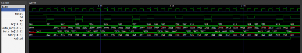
大功告成!
2条评论
I don't want to tell
Hi ,
I’m a first year CS student .
Can u plz help me with my manchester university assignment
Abbeyr
正愁看不懂这篇文章,找到个中文版,老哥牛批