使用Verilog搭建16位二进制加法器
Verilog是一种硬件描述语言,它通过文本形式描述数字系统硬件的结构或行为,常可以用来设计和测试逻辑电路,构建逻辑表达式以实现特定的逻辑功能。本节用它逐层递进实现16位二进制加法器的逻辑门级别结构设计,并完成相应的测试工作,最后分析了逻辑门的时延问题。
为了实现一个完整的加法器,首先需要了解二进制加法。为此,从1位二进制全加器开始设计,在此基础上组合实现4位加法器,测试无误后最终完成16位加法器的设计。
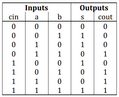
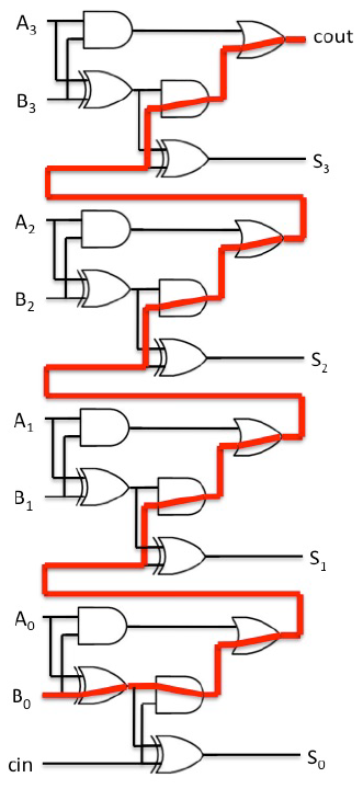
考虑1位全加器,有输入参数a,b,cin,其中a和b为二进制加数,cin为输入进位,若上一位有进位为1,否则为0。输出s,cout,其中s为相加结果,cout为进位输出,将a,b和cin进行二进制相加,末位保存在s中,若发生进位则cout为1,否则为0。(事实上,1个全加器还可以看作两个半加器的组合,在此略过不作解释)
在此基础上构建输入与输出对应关系的真值表。
理解真值表后,很容易设计出1位全加器的逻辑表达式:
s = (a ^ b) ^ cin ; cout = ((a ^ b) . cin) + (a . b) ;
在此基础上绘制出逻辑门原理图:
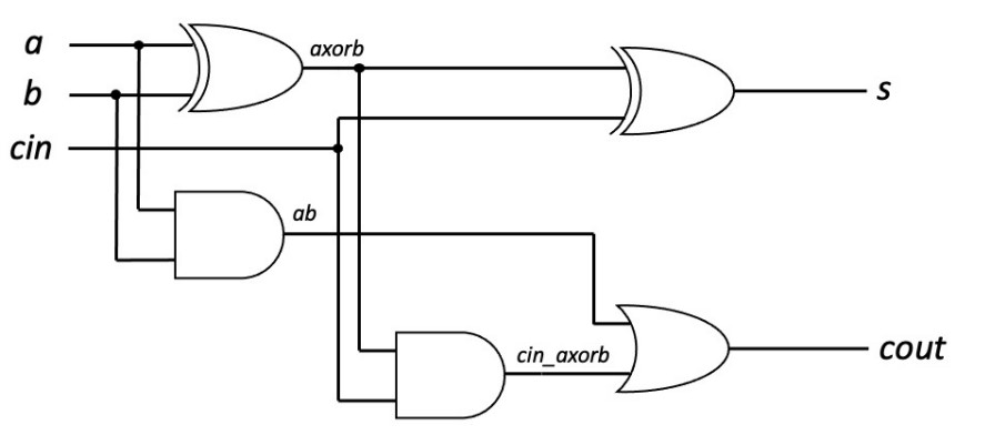
依据原理图编写Verilog全加器代码。(full_adder.v)
// Full adder design using verilog primitive gates

// All gates have a 1ns delay (#1 = 1ns)
`timescale 1ns/100ps

`default_nettype none

//Module definition

module full_adder(input  wire  a,
                  input  wire  b,
                  input  wire  cin,
                  output wire  s,
                  output wire  cout);

//Internal connections should be specified here
wire axorb;		// a^b
wire ab;		// a.b
wire cin_axorb;	// cin.(a^b)

// Sum logic for full adder s=(a^b)^cin
xor #1 gate1 (axorb, a, b);
xor #1 gate2 (s, cin, axorb);

// Carry logic for full adder cout=cin.(a^b) + a.b
and #1 gate3 (ab, a, b);
and #1 gate4 (cin_axorb, cin, axorb);
or  #1 gate5 (cout, cin_axorb, ab);

endmodule

`default_nettype wire
Verilog编写的构建以module为单位,定义输入、输出、中间变量,其中wire相当于物理连线,设计逻辑门,将对应的wire参数与逻辑门输出和输入相连即可,逻辑门编写无顺序要求,只关注连接的结构。代码中 #1 代表延迟1ns,以模拟真实逻辑门信号传递的延迟。
编写测试用例testbench。(full_adder_tb.v)
// Full adder testbench

// #1 = 1ns
`timescale 1ns/100ps

module full_adder_tb();

// Internal connections
reg a;
reg b;
reg cin;
wire s;
wire cout;

// Instantiate full adder as dut (device under test)

full_adder dut(a, b, cin, s, cout);

// Test vectors
// All combinations required
initial
 begin
  a = 0; b = 0; cin = 0;
  #100 a = 1;
  #100 a = 0; b = 1;
  #100 a = 1;
  #100 a = 0; b = 0; cin = 1;
  #100 a = 1;
  #100 a = 0; b = 1;
  #100 a = 1;
  #100 $finish; // exit the simulation
 end

// Save results as VCD file
initial
 begin
  $dumpfile("full_adder_tb_results.vcd");  // Save simulation waveforms in this file
  $dumpvars; // Capture all simulation waveforms
 end

endmodule
为了严谨性,需要测试所有输入情况的组合,共8种输入情况,每次间隔100ns显示结果。最终结果会以波形的形式输出并确认。
为了执行并验证Verilog代码,需要用到三个命令。
iverilog -y. -o full_adder_output full_adder_tb.v full_adder.v
vvp full_adder_output
gtkwave full_adder_tb_results.vcd
第一条指令编译代码并生成可执行文件,第二条指令执行并生成.vcd波形文件,第三条指令使用gtkwave工具将波形可视化。
输出结果如下图。
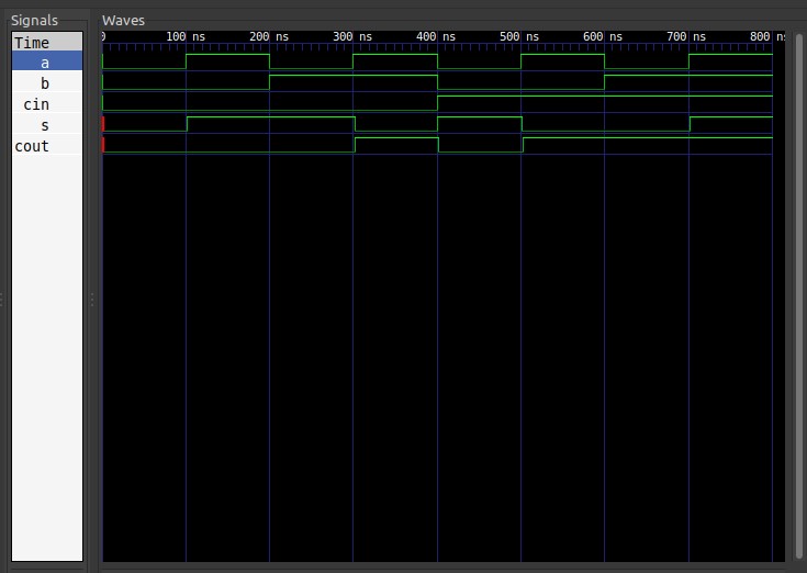
波形上沿表示对应变量值为1,下沿为0。通过示波器很容易验证全加器的正确性。
当把中间参数也显示出来并放大观察波形开头部分会发现一个奇怪的现象。
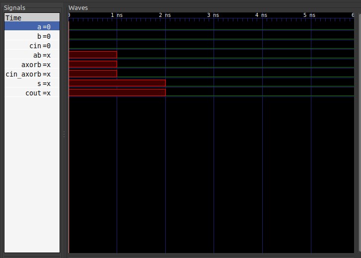
当观察门级延迟时,发现cout的输出延迟仅2ns,这与理论不符,cout的计算经过了3重逻辑门,累加应为3ns。
经过分析发现逻辑门计算也存在所谓的“短路现象”,即当已知某一输入参数的值后,若可直接得出输出值,则无需等待第二个参数。在本例中,由于一开始cin输入为0,导致与门gate4直接输出而不需要再等待a和b的异或结果,因此实际延迟仅2ns。
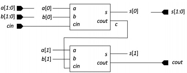
完成1位全加器设计后,在此基础上将全加器依次连接即可实现4位加法器。具体的,上一位的进位输出cout即为下一位的进位输入cin,其余输入输出保持一致。绘制出简易连接原理图如下。
据此编写4位加法器Verilog代码,其中只需引用之前的全加器模块并合理连接即可,无需再添加延迟因为延迟仅体现在底层逻辑门的信号传递中。
// 4-bit adder design using verilog primitive gates

`timescale 1ns/100ps

`default_nettype none

//Module definition

module adder_4bit(input  wire [3:0]  a,
                  input  wire [3:0]  b,
                  input  wire        cin,
                  output wire [3:0]  s,
                  output wire        cout);

//Internal carry connections
wire [2:0] c;	// carry out of three bits

// Instantiate 4 x full_adder
full_adder adder0 (a[0], b[0], cin,  s[0], c[0]);
full_adder adder1 (a[1], b[1], c[0], s[1], c[1]);
full_adder adder2 (a[2], b[2], c[1], s[2], c[2]);
full_adder adder3 (a[3], b[3], c[2], s[3], cout);

endmodule

`default_nettype wire
编写4位加法器测试用例,由于已经测试并确认过1位全加器,因此这里无需再测试所有的输入组合,而只需要测试各个输入位都正常且全加器连接处进位正常即可。
// 4-bit adder testbench

`timescale 1ns/100ps

module adder_4bit_tb();

// Internal connections
reg [3:0] a;
reg [3:0] b;
reg       cin;
wire [3:0] s;
wire cout;

// Instantiate adder_4bit as dut (device under test)

adder_4bit dut(a, b, cin, s, cout);

// Test vectors
initial
begin
// Using 14 test vectors the interconnect of the 4bit added can be verified

// Check all fulladders are connected to something, s=0 cout=0 not Xs
#100 a='b0000; b='b0000; cin=0;
// Check connections for a[0], b[0], cin, S[0], S=0001 cout=0
#100 a='b0001; b='b0000; cin=0;
#100 a='b0000; b='b0001; cin=0;
#100 a='b0000; b='b0000; cin=1;
// Check connection of carry out of the first adder
#100 a='b0001; b='b0001; cin=0;
// Check connections for a[1], b[1], c[1]
#100 a='b0010; b='b0000; cin=0;
#100 a='b0000; b='b0010; cin=0;
// 7 MORE TESTS
#100 a='b0010; b='b0010; cin=0;
#100 a='b0100; b='b0000; cin=0;
#100 a='b0000; b='b0100; cin=0;
#100 a='b0100; b='b0100; cin=0;
#100 a='b1000; b='b0000; cin=0;
#100 a='b0000; b='b1000; cin=0;
#100 a='b1000; b='b1000; cin=0;


// Connectivity tests completed.

// TESTS FOR FINDING MAXIMUM CARRY DELAY
// 2 test vectors required - one to initialise followed by the 2nd to exercise
// the critical path
#100 a='b0000; b='b0000; cin=0;
#100 a='b1111; b='b0000; cin=1;

// delay for end of wave traces to be visible
#100 $finish; // exit the simulation
end


// Save results as VCD file
initial
 begin
  $dumpfile("adder_4bit_tb_results.vcd");  // Save simulation waveforms in this file
  $dumpvars; // Capture all simulation waveforms
 end

endmodule
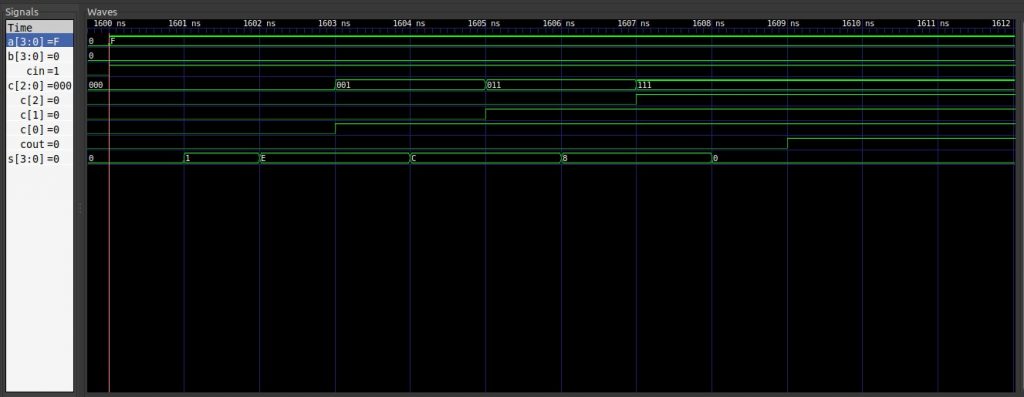
这里不再贴出波形结果,仅讨论一下最大延时问题。为了达成最大延迟必须确保全加器中的gate4即输出cin_axorb的与门避免触发短路逻辑,为此a与b的异或结果必须为1,每一位输入均满足 a≠b ,并且进位输入cin为1,即每一位始终有进位出现。
在这种情况下,4位加法器cout的最大延时为9ns,具体的,在第1ns时所有4个加法器同时完成了a异或b的运算,等待前一个加法器的cin输入,之后从低位到高位每个加法器依次延迟2ns(gate4 和 gate5的延迟)并传递进位值cout,最终总延时 1 + 2 * 4 = 9ns。
最后让我们实现16位加法器,与之前的层级组合方式类似,16位加法器由4个4位加法器依次连接组合而成,不再过多解释。
16位加法器设计代码:
// 16-bit adder design using verilog primitive gates

`timescale 1ns/100ps
`default_nettype none

module adder_16bit(input  wire [15:0]  a,
	               input  wire [15:0]  b,
				   input  wire         cin,
				   output wire [15:0]  s,
				   output wire         cout);

//Internal carry connections
wire [3:0] c;	//carry out of 4 4bit adders

// Instantiate 4 x adder_4bit
adder_4bit adder4b0 (a[3:0],   b[3:0],   cin,  s[3:0],   c[0]);
adder_4bit adder4b1 (a[7:4],   b[7:4],   c[0], s[7:4],   c[1]);
adder_4bit adder4b2 (a[11:8],  b[11:8],  c[1], s[11:8],  c[2]);
adder_4bit adder4b3 (a[15:12], b[15:12], c[2], s[15:12], cout);

endmodule

`default_nettype wire
16位加法器测试代码:
// 16-bit adder testbench

// #1 = 1ns
`timescale 1ns/100ps

module adder_16bit_tb();

// Internal connections
reg [15:0]  a;
reg [15:0]  b;
reg         cin;
wire [15:0] s;
wire        cout;

// Instantiate adder_16bit as dut (device under test)

adder_16bit dut(a, b, cin, s, cout);

// Test vectors
initial
begin
// 38 test vectors required for connectivity tests
// Check all adders are connected to something, S=0 cout=0 not Xs
#100 a=16'h0000; b=16'h0000; cin=0;
//Check connections for A[0], B[0], Cin, S[0], S=0001 cout=0
#100 a=16'h0001;
#100 a=16'h0000; b=16'h0001;
#100 a=16'h0000; b=16'h0000; cin=1;
//Check connections for  A[1], B[1], S[1]
#100 a=16'h0002; b=16'h0000; cin=0;
#100 a=16'h0000; b=16'h0002;
//Check connections for  A[2], B[2], S[2]
#100 a=16'h0004; b=16'h0000;
#100 a=16'h0000; b=16'h0004;
//Check connections for  A[3], B[3], S[3]
#100 a=16'h0008; b=16'h0000;
#100 a=16'h0000; b=16'h0008;
//Check connection of carry out of the first 4bit adder in to 2nd 4-bit adder
#100 a=16'h0008; b=16'h0008;
// Continue with the same pattern shown above
// 27 test vectors including the carry out
// -------------------------------------------------
//check connections for A[7:4], B[7:4], S[7,4]
#100 a=16'h0010; b=16'h0000;
#100 a=16'h0000; b=16'h0010;
#100 a=16'h0020; b=16'h0000;
#100 a=16'h0000; b=16'h0020;
#100 a=16'h0040; b=16'h0000;
#100 a=16'h0000; b=16'h0040;
#100 a=16'h0080; b=16'h0000;
#100 a=16'h0000; b=16'h0080;
//Check connection of carry out of the 2nd 4bit adder in to 3rd 4-bit adder
#100 a=16'h0080; b=16'h0080;
//check connections for A[11:8], B[11:8], S[11:8]
#100 a=16'h0100; b=16'h0000;
#100 a=16'h0000; b=16'h0100;
#100 a=16'h0200; b=16'h0000;
#100 a=16'h0000; b=16'h0200;
#100 a=16'h0400; b=16'h0000;
#100 a=16'h0000; b=16'h0400;
#100 a=16'h0800; b=16'h0000;
#100 a=16'h0000; b=16'h0800;
//Check connection of carry out of the 3rd 4bit adder in to 4th 4-bit adder
#100 a=16'h0800; b=16'h0800;
//check connections for A[15:12], B[15:12], S[15:12]
#100 a=16'h1000; b=16'h0000;
#100 a=16'h0000; b=16'h1000;
#100 a=16'h2000; b=16'h0000;
#100 a=16'h0000; b=16'h2000;
#100 a=16'h4000; b=16'h0000;
#100 a=16'h0000; b=16'h4000;
#100 a=16'h8000; b=16'h0000;
#100 a=16'h0000; b=16'h8000;
//Check connection of carry out of the 4th 4bit adder in to cout
#100 a=16'h8000; b=16'h8000;


// Connectivity tests completed.

// TESTS FOR FINDING MAXIMUM CARRY DELAY
// 2 test vectors required - one to initialise followed by the 2nd to exercise
// the critical path
#100 a=16'h0000; b=16'h0000; cin=0;
#100 a=16'hFFFF; b=16'h0000; cin=1;


// -------------------------------------------------
// delay for end of wave traces to be visible
#100 $finish;
end

// Save results as VCD file
initial
 begin
  $dumpfile("adder_16bit_tb_results.vcd");  // Save simulation waveforms in this file
  $dumpvars; // Capture all simulation waveforms
 end

endmodule
其中最大延迟 delay = 1 + 2 * 16 = 33ns。
采用以上方法实现的加法器称作“行波进位加法器”,其短板就在于最大延迟随着计算位数的增加而增大。事实上,为了优化加法器运行效率,缩短最大延迟,可以采用另一种设计方法“超前进位加法器”。简单来说,超前进位加法器在计算每一位的进位时,并非依赖前一位的进位结果来计算自己的输出,而直接根据之前所有位的a和b的输入计算当前进位。这么做显然增加了电路设计的复杂度,但可以有效降低最大延迟。对于“超前进位加法器”,计算分为三步,首先计算每一位a与b、a或b的值,然后据此计算每一位进位输出,最后是每一位的求和输出。其最大延迟仅1+2+1=4ns。然而当所需计算位数增加时,电路的复杂度往往超出可接受的范围,因此可以通过多个“超前进位加法器”的并列组合实现更多位数的加法器。
The end~
滑稽:实现64位二进制加法器。
module adder_64bit(input wire [63:0] a, input wire [63:0] b, input wire cin, output reg [63:0] sum, output reg carry);
always @ (*)
        {carry, sum} = a + b + cin;
endmodule
4条评论
西云
大佬牛逼,学到了。感谢感谢!
Makinohara
太强了,大佬
liu
学长可以问一下你的wx🐎
RyanXin
欢迎随时邮件联系哦!